- 您现在的位置:买卖IC网 > Sheet目录3872 > PIC16C57C-04/SP (Microchip Technology)IC MCU OTP 2KX12 28DIP
2002 Microchip Technology Inc.
Preliminary
DS30453D-page 11
PIC16C5X
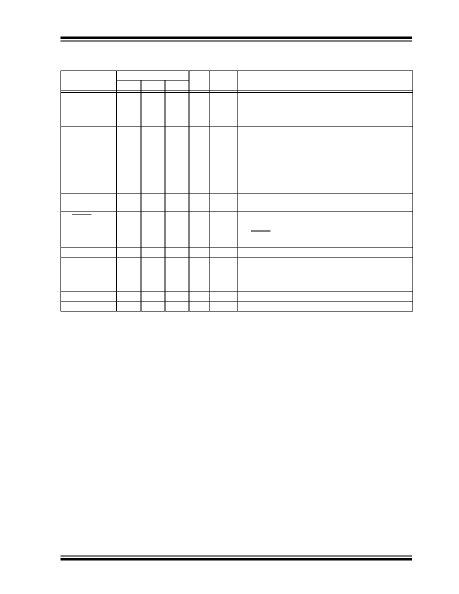
TABLE 3-1:
PINOUT DESCRIPTION - PIC16C54, PIC16CR54, PIC16C56, PIC16CR56, PIC16C58,
PIC16CR58
Pin Name
Pin Number
Pin
Buffer
Description
DIP
SOIC
SSOP Type
Type
RA0
RA1
RA2
RA3
17
18
1
2
17
18
1
2
19
20
1
2
I/O
TTL
Bi-directional I/O port
RB0
RB1
RB2
RB3
RB4
RB5
RB6
RB7
6
7
8
9
10
11
12
13
6
7
8
9
10
11
12
13
7
8
9
10
11
12
13
14
I/O
TTL
Bi-directional I/O port
T0CKI
3
I
ST
Clock input to Timer0. Must be tied to VSS or VDD, if not in
use, to reduce current consumption.
MCLR/VPP
4
I
ST
Master clear (RESET) input/programming voltage input.
This pin is an active low RESET to the device. Voltage on
the MCLR/VPP pin must not exceed VDD to avoid unin-
tended entering of Programming mode.
OSC1/CLKIN
16
18
I
ST
Oscillator crystal input/external clock source input.
OSC2/CLKOUT
15
17
O
—
Oscillator crystal output. Connects to crystal or resonator
in crystal Oscillator mode. In RC mode, OSC2 pin outputs
CLKOUT, which has 1/4 the frequency of OSC1 and
denotes the instruction cycle rate.
VDD
14
15,16
P
—
Positive supply for logic and I/O pins.
VSS
5
5,6
P
—
Ground reference for logic and I/O pins.
Legend: I = input, O = output, I/O = input/output, P = power, — = Not Used, TTL = TTL input, ST = Schmitt Trigger
input
发布紧急采购,3分钟左右您将得到回复。
相关PDF资料
PIC16LF628A-I/SO
IC MCU FLASH 2KX14 EEPROM 18SOIC
PIC16C55A-20/SO
IC MCU OTP 512X12 28SOIC
PIC24F16KA101-I/MQ
IC PIC MCU FLASH 16KB 20-QFN
PIC16F627-04/SO
IC MCU FLASH 1KX14 COMP 18SOIC
PIC16C58B-20I/P
IC MCU OTP 2KX12 18DIP
PIC24FJ16GA002-I/SS
IC PIC MCU FLASH 16K 28-SSOP
PIC16C55A-04I/SO
IC MCU OTP 512X12 28SOIC
PIC16CR77-I/ML
IC PIC MCU 8KX14 44QFN
相关代理商/技术参数
PIC16C57C-04/SP
制造商:Microchip Technology Inc 功能描述:IC 8BIT CMOS MCU 16C57 SDIL28
PIC16C57C-04/SP
制造商:Microchip Technology Inc 功能描述:Microcontroller IC Number of I/Os:20
PIC16C57C-04/SS
功能描述:8位微控制器 -MCU 3KB 72 RAM 20 I/O RoHS:否 制造商:Silicon Labs 核心:8051 处理器系列:C8051F39x 数据总线宽度:8 bit 最大时钟频率:50 MHz 程序存储器大小:16 KB 数据 RAM 大小:1 KB 片上 ADC:Yes 工作电源电压:1.8 V to 3.6 V 工作温度范围:- 40 C to + 105 C 封装 / 箱体:QFN-20 安装风格:SMD/SMT
PIC16C57C-04E/P
功能描述:8位微控制器 -MCU 3KB 72 RAM 20 I/O RoHS:否 制造商:Silicon Labs 核心:8051 处理器系列:C8051F39x 数据总线宽度:8 bit 最大时钟频率:50 MHz 程序存储器大小:16 KB 数据 RAM 大小:1 KB 片上 ADC:Yes 工作电源电压:1.8 V to 3.6 V 工作温度范围:- 40 C to + 105 C 封装 / 箱体:QFN-20 安装风格:SMD/SMT
PIC16C57C-04E/SO
功能描述:8位微控制器 -MCU 3KB 72 RAM 20 I/O RoHS:否 制造商:Silicon Labs 核心:8051 处理器系列:C8051F39x 数据总线宽度:8 bit 最大时钟频率:50 MHz 程序存储器大小:16 KB 数据 RAM 大小:1 KB 片上 ADC:Yes 工作电源电压:1.8 V to 3.6 V 工作温度范围:- 40 C to + 105 C 封装 / 箱体:QFN-20 安装风格:SMD/SMT
PIC16C57C-04E/SP
功能描述:8位微控制器 -MCU 3KB 72 RAM 20 I/O RoHS:否 制造商:Silicon Labs 核心:8051 处理器系列:C8051F39x 数据总线宽度:8 bit 最大时钟频率:50 MHz 程序存储器大小:16 KB 数据 RAM 大小:1 KB 片上 ADC:Yes 工作电源电压:1.8 V to 3.6 V 工作温度范围:- 40 C to + 105 C 封装 / 箱体:QFN-20 安装风格:SMD/SMT
PIC16C57C-04E/SS
功能描述:8位微控制器 -MCU 3KB 72 RAM 20 I/O RoHS:否 制造商:Silicon Labs 核心:8051 处理器系列:C8051F39x 数据总线宽度:8 bit 最大时钟频率:50 MHz 程序存储器大小:16 KB 数据 RAM 大小:1 KB 片上 ADC:Yes 工作电源电压:1.8 V to 3.6 V 工作温度范围:- 40 C to + 105 C 封装 / 箱体:QFN-20 安装风格:SMD/SMT
PIC16C57C-04I/P
功能描述:8位微控制器 -MCU 3KB 72 RAM 20 I/O RoHS:否 制造商:Silicon Labs 核心:8051 处理器系列:C8051F39x 数据总线宽度:8 bit 最大时钟频率:50 MHz 程序存储器大小:16 KB 数据 RAM 大小:1 KB 片上 ADC:Yes 工作电源电压:1.8 V to 3.6 V 工作温度范围:- 40 C to + 105 C 封装 / 箱体:QFN-20 安装风格:SMD/SMT